
Tesla and Apple cut into glass substrates, and the battle continues to rise
Tesla and Apple are considering introducing glass substrates into the next generation of semiconductors, and have recently been in contact with related manufacturers and equipment suppliers.
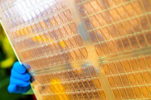
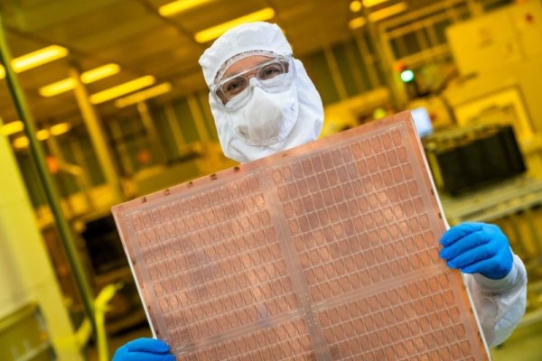
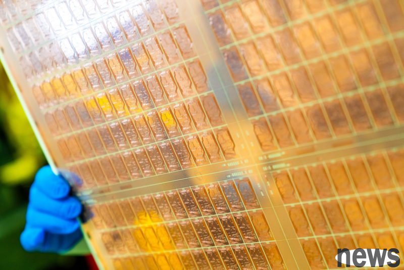
As the demand for artificial intelligence and high-efficiency computing continues to rise, glass substrates are regarded as an important solution to break through existing packaging restrictions. Currently, mainstream PCB substrates are mostly made of glass fiber and resin mixed with copper layer and solder layer. However, organic substrates are very sensitive to heat and can easily lead to degradation of wafer performance when temperatures are too high, which is difficult to accept for AI and HPC (high-performance computing) applications that emphasize accuracy. Although the industry has used a variety of technologies to control wafer temperature, the effect is still limited.
In contrast, glass substrates can withstand higher operating temperatures, allowing wafers to maintain maximum performance over long periods of time. At the same time, its surface is flatter (less curved) and can be engraved with high precision, reducing the distance between components and further improving circuit density.
According to industry news, Tesla is evaluating the high computing needs of applying glass substrates to next-generation self-driving (FSD) chips to support the high computing needs of automatic driving of electric vehicles and humanoid robots. Apple may introduce it to ASIC or iPhone and MacBook's self-developed chips and further extend it to AI servers and data centers. It is worth noting that Apple partner Broadcom has invested heavily in the glass substrate field and completed prototype testing, which also increases the possibility of actual adoption.
Although the glass substrate exhibits significant potential, there are still challenges in distance production. The first is the processing difficulty, such as the processing cost and yield problems of TGV (through-Glass Via). The second is the supply chain, including glass panels that need to be extra cautious during the handling and cutting process, resulting in an increase in manufacturing and testing costs. Therefore, although the industry has started experiments and cooperation, it is still mostly at the stage of technical verification and small-scale introduction.
At present, manufacturers such as Intel, AMD, Samsung Electronics, Amazon (AWS), and Broadcom are all promoting related research and development and introduction plans, indicating that glass substrates are gradually moving towards industry trends and are expected to become an important option for the next generation of chip packaging.
Glass Substrates Are Beginning to Draw Big Tech Interest, With Apple and Tesla Reportedly Lining Up for Adoption in Next-Gen Chips