
From the consumer market to the advanced semiconductor packaging, glass is turned into substrate material and red fried chicken
In an era of rising demand for artificial intelligence (AI) and high-performance computing (HPC), semiconductor industries are undergoing unprecedented technological innovation. Among them, the status of glass materials is rising from past consumer consumables to the core of advanced packaging technology, and is expected to become the key foundation for wafer connection, signal transmission and even photon guidance. The market report released by IDTechEx, an international research organization, "Glass in Semiconductors 2026-2036: Applications, New Technology and Market Insights" explored this trend in depth and predicted the broad prospects of glass in the semiconductor field.
AI and HPC drive glass reversing
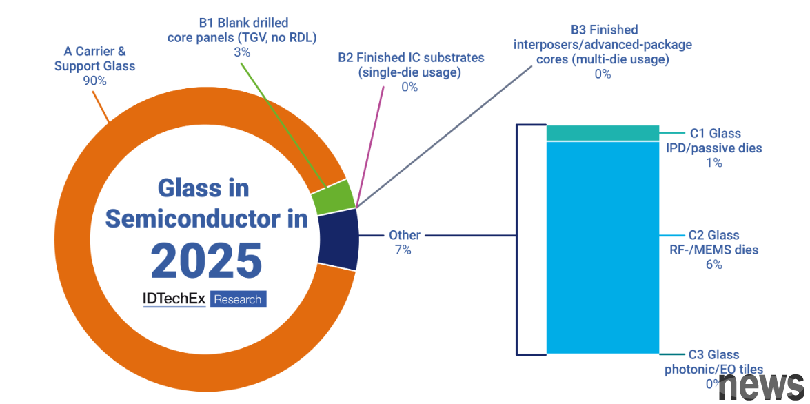
The reason why glass can meet this role change is that the main catalyst behind it is the increasingly severe frequency width and power density requirements of AI and HPC devices. Modern training accelerators require thousands of high-speed I/O convexities, as well as a power supply network that can handle hundreds of acres of current with minimal messaging. The main material for the past two decades has been organic base plates, but it is difficult to maintain the required flatness and through-hole density when facing these continuous growth needs. Although silicon intermediary layers can provide more detailed wiring, their high price and limited panel size limit their application scope.
Therefore, between the organic base plate and the silicon intermediary layer, glass cleverly found its positioning. Thermal expansion (CTE) of glass is one level lower than silicon, showing its superior performance in high-speed signal transmission. What is even more remarkable is that the potential of large-panel processing from the LCD industry in the past represents that a single sheet of glass substrate can reach half a meter square. With the increase in yield, its cost is expected to be closer to high-level organic materials.
With the surge in demand for AI and HPC, each layer in the package stack must bear higher current, more I/O, and faster signal speeds. This makes it difficult for traditional organic base plates and even the first generation of silicon intermediary layers to match. It is under these pressures that the glass core substrate and large-panel glass intermediary layer have quickly moved towards commercialization from the past.
Double-engine integration of high-frequency communication and photons expands the marketIn addition to meeting the computing packaging needs, glass has low dielectric consumption and optical transparency, and high frequency and photon integration provide it with a second growth engine. Because in the Ka frequency segment and above, the insertion of the glass microstrip is only half the equivalent organic circuit. This makes it an ideal choice for high-frequency applications such as 5G/6G communication.
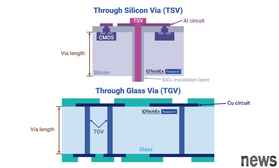
Silicon photon integration brings additional power to the peripheral market. Co-packaged optics (CPO) The purpose is to move the optical fiber connection from the front panel of the switch to a substrate only a few millimeters away from the switch ASIC. Engineering glass can not only carry the electric redistribution layer, but also accommodate low-energy light-consuming waveguides, thereby simplifying the standard process and eliminating the expensive silicon photon intermediary layer. Due to the Through-glass via (TGV) technology used for transmitting frequency, vertical optical guides can be created, and a single glass core can simultaneously support the transfer amplifier, laser driver and optical waveguide itself. This fusion of electronics and photon routing just happens to unleash the strength of glass, pushing its potential market into a broader field beyond traditional electronic packaging.
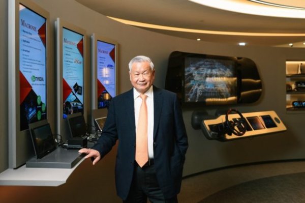
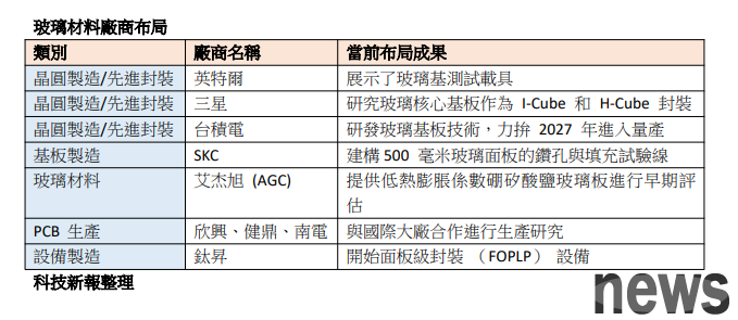
At present, the leading device manufacturers and material suppliers in the industry have publicly invested in the research and development of this technology. Intel, for example, showed glass-based test loads online in its exploratory production in Arizona. Samsung Electronics is also exploring glass core substrates as potential options for its I-Cube and H-Cube packaging. Wei Zhejia, chairman of the Crystal OEM, has also proved that it is developing glass substrate technology and striving to enter mass production in 2027. FOPLP (fan-out panel-level packaging) plus TGV diamond holes will be the technical key. As for, SKC, a large Korean substrate manufacturer, has installed a diamond hole and fill test line for 500mm glass panels. Ai Jiexu (AGC), a major glass manufacturer, provides borosilicate salt glass plates with low thermal expansion for early evaluation.
For Taiwanese manufacturers, in addition to the traditional PCB factories, including Xingxing, Jianding, Nan Electric, and other manufacturers who can benefit from the emergence of new business machines, the equipment manufacturer Liusheng focuses on FOPLP processes, providing laser printing, cutting, electrical cleaning, laser decoction, ABF diamond holes and other full-process equipment, supporting large-size panels from 300×300mm to 700×700mm. The equipment adopts modular design and high-precision control, which not only greatly improves production capacity, but also can handle substrates up to 16mm curved. Currently, it has been proven to ship the large-scale panel manufacturer of Taiwan, STMicroelectronic fan-out panel-level packaging (FOPLP) equipment. In addition, it also reported that it received orders for Intel's advanced packaging new line equipment, and the launch of the fourth season of the regulations will begin. At the same time, there are also news about contacting Broadcom to negotiate advanced packaging equipment orders, which is expected to promote operation.
 Supply chain ecosystem determines the success of glass
Overall, the key to glass moving from trial production lines to mass production in the future is not the availability of raw materials, but more importantly, the establishment of new ecological systems such as laser diamond holes, copper filling, panel processing and design automation. In addition, yield learning curves, hole filling reliability, panel curves and design tools maturity will determine whether glass can meet the cost targets set by the system integration merchandise.. What is also important is the competitive dynamic between glass and silicon and improved organic materials, because the wafer foundry is promoting hybrid wafer redistribution technology, which reduces the advantages of glass in characteristic size. At the same time, layer plate suppliers are also developing next-generation ABF cores that have lower roughness and better thermal expansion matching.
Generally speaking, driven by AI and HPC technology, glass materials are moving from behind the screen to the forefront of semiconductor packaging. With its unique physical and chemical characteristics, it is expected to have an irreplaceable role in the next generation of high-performance chip packaging, high-frequency communication and photon integration. Although the industry is still facing challenges in supply chain establishment and technological maturity, its development potential has been widely recognized by the industry.